Written in LUV, runs on light
LUV (Light Unified Virtualizations) is the programming language for QLT's photonic quantum processors. Write a short program describing what you want the chip to do — LUV compiles it into the exact voltages, phase masks, and detector contracts your hardware needs. Think of it like CUDA for GPUs, but for photonic quantum chips: a thin, precise layer between your intent and the physics.
Why does a photonic chip need its own language?
Without LUV
NumPy spaghetti that breaks between chips
Today, most photonic processors are controlled by one-off Python scripts. An engineer hand-computes MZI phases in NumPy, manually maps them to DAC voltages, writes custom SPAD readout parsers, and hopes the simulation matches reality. Every chip needs different code. Nothing is portable. There's no way to tell which numbers came from simulation vs. real measurements. And when you move from an 8-mode chip to a 64-mode chip, you start from scratch.
With LUV
Write once — the compiler handles the physics
LUV gives you 6 lines of code that compile to any QLT chip from GEMINI (2 modes) through LOTUS (512 modes). The luvc compiler decomposes your intent into exact MZI phases, crosstalk-corrected DAC voltages, spectral holograms, and heralded shot contracts — all tagged with honesty labels so you always know what's simulated vs. what's measured. The same program runs on any chip in the ladder.
From 6 lines of code to photons in 5 stages
① You write a .luv file — declaring which chip, which field arithmetic, and what gates/measurements you want. This is the programmer-facing surface.
② luvc build compiles to QIL IR — the compiler constant-folds all Galois field expressions, validates your field/chip compatibility, and lowers every statement to the QIL Intermediate Representation (a JSON bundle). No second semantics — everything the language can express must lower to IR.
③ Three hardware artifacts are produced — simultaneously: dac.voltages[32] (crosstalk-corrected heater voltages for the AD5372 DAC, via inverse thermal matrix G⁻¹), qfp_schedule[] (ordered unitary/phase-mask/permutation steps for the spectral processor), and a shot_contract (which SPADs to arm, what herald pattern to accept, post-selection probability).
④ The FPGA consumes these artifacts — the firmware's SPI master writes DAC voltages to 32 TiN heaters (54 µs refresh), the TDC captures SPAD clicks at 64 ps resolution, and the BRAM feedforward LUT fires TFLN switches within 11.2 ns of a herald detection. The grid_valid hardware interlock refuses to issue opcodes until the comb servo is locked.
⑤ luvc run validates the entire chain — the digital-twin simulator (galois/JAX + Mr Mustard + The Walrus) executes the same program against a physics-accurate model. The simulator is the FPGA behavioral specification — when firmware exists, its acceptance test is byte-level agreement with luvc run.
What makes LUV different from every other quantum language
01 Every statement maps to something the chip can physically do
LUV is a device language ● not a universal circuit model. There are no abstract gates. mesh dft 8 becomes 28 real MZI phase settings. gate F_d 10 becomes a spectral phase mask on a physical frequency comb. shot seed 7 fires an actual pump laser and reads real SPAD detectors. If a statement doesn't lower to hardware, it doesn't compile.
02 One line of code changes the entire physics stack
Write field 1 and you're in GF(2) ● qubits on GEMINI's 8-mode Clements mesh with 32 DAC channels. Change it to field 8 and you're in GF(256) ● 256-dimensional qudits on THETA's 7-tile module with 4,096 heater channels. The compiler handles everything: field arithmetic, error correction codes, gate decompositions, DAC bank sizing, and detector configuration. You just change one number.
03 The simulator is the hardware specification
Most quantum companies build hardware first, then write software to control it. QLT does the opposite: the luvc run digital twin defines exactly what the FPGA firmware must reproduce ● stall semantics, detection patterns, feedforward timing, measure destructuring. When silicon arrives, its acceptance test is byte-level agreement with the simulation. The software isn't approximating the hardware. It's specifying it.
04 11.2 nanoseconds from detection to correction
When a photon hits the SPAD, the FPGA has 11.2 ns to read the result, look up the correction in BRAM, and fire the TFLN electro-optic switch ● all while the entangled partner photon is still traveling through a 3.5 ns delay spiral. LUV's when keyword doesn't just describe conditional logic. It describes a nanosecond-scale physical feedback loop that rewrites the photonic circuit between two entangled photons.
05 Every number tells you where it came from
LUV enforces machine-readable honesty. Every output carries a provenance tag ● [simulated] for digital-twin numbers, [model] for engineering approximations, [designed/target] for unverified design intent. These are structural JSON fields, not code comments. Downstream tooling can programmatically refuse to mix simulation data with real measurements. No other quantum language enforces this.
06 Error correction is built into the type system
Reed-Solomon codes aren't bolted on after the fact ● they're a direct consequence of the field declaration. field 4 gives you GF(16) and automatically enables RS(15,11). field prime 11 gives you GF(11) and RS(10,8). rs_encode and rs_decode are first-class verbs that compile to on-chip encoding before photonic gates and syndrome checking after measurement. QEC lives in the language, not in a library.
07 Six lines of code. 28 heater phases. One photon.
A complete LUV program is six lines. The compiler turns it into 28 Clements-decomposed MZI phases, maps them through a 32×32 thermal crosstalk inverse, encodes them as 24-bit AD5372 SPI frames, fires the pump laser, arms 24 SPAD detectors, applies torontonian threshold sampling, and returns a heralded photon detection event ● with full honesty tagging on every intermediate result. You wrote six lines. The toolchain did the rest.
A programming language built for light
LUV's central insight: the correct abstraction for programmable photonic processors is finite-field arithmetic acting on an array of optical modes. Every chip in the QLT ladder natively realizes a Galois field — GF(2) on GEMINI, GF(11) on SOLAR, GF(2⁴) through GF(2⁹) on GALAXY through LOTUS. Every physical control primitive — an MZI phase rotation, a frequency-bin permutation, a spectral hologram — is the image of an algebraic verb under a fixed lowering map.
This means one field declaration simultaneously fixes your arithmetic, your Reed-Solomon error correction, your qudit dimension, your legal chip targets, and your DAC bank size. Change field 1 to field 6 and the compiler automatically adjusts from GEMINI's 28-phase Clements mesh to NOVA's 2,016-cell QFP with 2,048 heater channels — same language, same toolchain, completely different hardware.
No second semantics
Anything LUV expresses must lower to QIL IR 0.1.0. The IR — not the surface syntax — is the contract with the execution layer. galois/JAX remain the simulation engine; LUV is the programmer-facing skin. The compile spine: parse_luv → lower_to_ir → decompose_program → dac_schedule.
Machine-readable provenance
Every compiled artifact carries [simulated], [model], or [designed/target] labels as JSON fields — not comments — so downstream tooling can refuse to mix grades. This is whitepaper principle P3 implemented as schema, not commentary.
APL-flavored verbs for photonic hardware
UTF-8 text, one statement per line, # comments. Unicode glyphs and ASCII digraphs are interchangeable — luvc fmt canonicalizes to glyphs.
| Glyph | ASCII | Meaning |
|---|---|---|
| ← | <- | binding |
| ⊕ | (+) | GF add (XOR in char-2) — elementwise on arrays |
| ⊗ | (*) | GF multiply — elementwise on arrays |
| ⌽ | (<<) | cyclic rotate (dyadic: k ⌽ v) |
| ⍉ | (T) | matrix transpose (monadic) |
target · field
target GEMINI sim selects chip and backend (sim or qpu). field 8 declares GF(2⁸) — fixing arithmetic, RS codes, qudit dimension, and legal chip targets in one line.
mesh · gate · hologram
mesh dft 8 → Clements synthesis. gate F_d 10 → QFP unitary. hologram e8 17 → E8 root phase mask. shift 3 → bin-grid permute.
shot · measure · when
shot seed 7 requests a heralded sample [simulated]. measure m0 destructures into a GF symbol. v0.3 when adds post-measure feedforward at the ~11.2 ns herald tier.
TDM holograms and feedforward
hologram time [r0 ; r1 ...] lowers to a TDMSequence — one phase-mask step per time slot for rank-2 freq×time programs. when m0 = K shift 1 lowers to a Feedforward IR op kept out of the pre-shot schedule; the runtime fires matching conditions against decoded measures and logs the [model] 11.2 ns budget.
Also: rs_encode / rs_decode, iota, emit, hologram amp [...] phase [...] for post-selected complex masks.
From .luv to hardware artifacts
luvc build emits one .qil.json bundle. Three hardware-facing artifacts are produced simultaneously.
.luv source
Line-oriented program with field, mesh/gate/hologram, shot.
luvc compile
Parse + constant fold GF expressions. Lower to QIL IR 0.1.0. Decompose into Clements phases, QFP schedule, DAC vector.
Three artifacts
28 Clements phases → crosstalk-corrected 0–5 V words for AD5372 [model]
Ordered unitary / phase_mask / amp_phase_mask / permute steps [simulated]
SPAD pattern + comb_lock gate + post-selection probability [simulated]
luvc run
Digital twin execution: run_gemini_shot (mesh path) or run_freqbin_shot (gate-only path). Acceptance test for future FPGA firmware = agreement with luvc run.
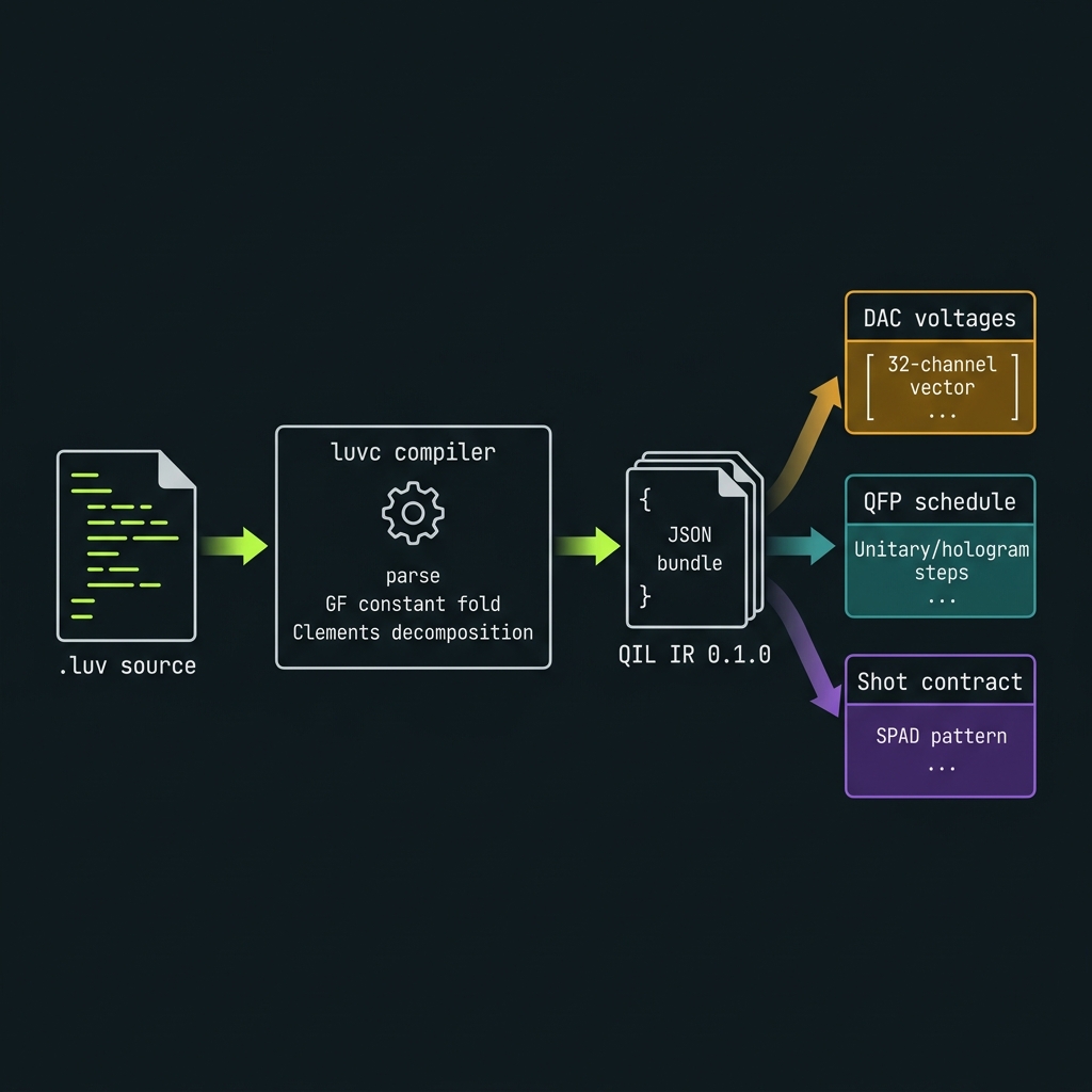 Pipeline
.luv source through luvc to three hardware-facing artifacts.Programs that run today [simulated]
Runnable examples in _qil/luv/examples/. Build with luvc build, execute with luvc run.
8-mode DFT mesh + heralded shot on GEMINI
luv 0.1
target GEMINI sim
field 1                  # GF(2) — GEMINI baseline

mesh dft 8               # 8-mode DFT -> 28 Clements phases -> 32-ch DAC
shot seed 7              # torontonian SPAD sample [simulated]
Line-by-line:
luv 0.1 — declares the language version (v0.1). The compiler uses this to know which keywords are legal.
target GEMINI sim — tells the compiler which chip to target (GEMINI) and which backend to use (sim = digital-twin simulation, vs qpu for real hardware). This sets the chip's mode count, detector layout, and DAC channel map.
field 1 — the number 1 is the exponent k in GF(2k). So field 1 = GF(21) = GF(2), which means each qudit has 2 levels (a qubit). On GEMINI, this maps to dual-rail path encoding with two waveguides per qubit. If you wrote field 4, you'd be targeting GF(24) = GF(16) = GALAXY's 16-bin frequency comb.
mesh dft 8 — synthesize a discrete Fourier transform across 8 optical modes. The compiler decomposes this 8×8 unitary into 28 individual MZI (Mach–Zehnder interferometer) phase settings using the Clements algorithm, then maps those 28 phases onto GEMINI's 32-channel AD5372 DAC with crosstalk correction.
shot seed 7 — fire one heralded single-photon detection event. seed 7 is the random seed for the simulation's torontonian sampler (which models what GEMINI's SPAD detectors would click). On real hardware, this would trigger the pump laser, wait for a herald click, and record the output pattern.
RS(10,8) encode → gate → shot → measure → decode
luv 0.2
target SOLAR sim
field prime 11

let msg ← [3 1 4 1 5 9 2 6]
let cw  ← rs_encode msg
let back ← rs_decode cw          # syndrome check lands in rs_ok["back"]

gate F_d 10
shot seed 3
measure m0
Line-by-line:
field prime 11 — SOLAR is the only chip that uses a prime field instead of a power-of-2 field. The keyword prime tells the compiler to use GF(11) (integers mod 11) instead of GF(2k). The number 11 is the prime modulus. SOLAR's 10-tooth frequency comb has 10 bins numbered 0–9, and the 11th element (0) wraps around — so arithmetic is modular division over 11 values.
let msg ← [3 1 4 1 5 9 2 6] — bind an array of 8 GF(11) symbols (the digits of pi!) to the variable msg. The arrow ← is LUV's assignment operator (APL-style). Each number must be 0–10 to be valid in GF(11).
rs_encode msg — apply Reed–Solomon encoding to the 8-symbol message, producing a 10-symbol codeword (RS(10,8) adds 2 parity symbols). This is how LUV does quantum error correction — the RS code protects the data across the comb's frequency bins.
rs_decode cw — decode the codeword back, checking for errors. The syndrome result (pass/fail) is stored in rs_ok["back"] — a JSON field the runtime can inspect.
gate F_d 10 — apply the quantum Fourier transform gate (F_d) over dimension 10 (SOLAR's 10 frequency bins). This is a QFP (Quantum Fourier Processor) unitary that rotates the quantum state across all 10 comb teeth simultaneously. The compiler lowers this to a spectral phase mask on SOLAR's AWG.
shot seed 3 — fire one heralded detection event (seed 3 for the random number generator). On SOLAR, this means pumping the 10-tooth comb and detecting which frequency bin clicks.
measure m0 — destructure the SPAD click pattern into a GF(11) symbol stored in variable m0. The detector saw bin #k click → m0 now holds the integer k. This is the measurement result you can branch on.
TDM hologram + post-measure feedforward
when m0 = 0 shift 1      # if the click landed in bin 0, advance the grid
when m0 = 5 gate Z_d 10  # if it landed in bin 5, apply a Z_d frame
Line-by-line:
when m0 = 0 shift 1 — this is a conditional feedforward instruction. After measuring, if the result m0 equals 0 (meaning the photon was detected in frequency bin 0), then execute shift 1 — which advances the frequency-bin grid by 1 position. This happens in hardware at the ~11.2 ns feedforward tier: the SPAD fires → TDC timestamps it → FPGA looks up the action in a BRAM table → TFLN electro-optic switch shifts the grid. The photon is held in a delay spiral during this entire ~11 ns loop.
when m0 = 5 gate Z_d 10 — if the measurement result was 5 (bin 5 clicked), apply a Z_d phase gate across all 10 frequency bins. Z_d is the diagonal phase gate in dimension d — it applies a phase rotation of e^(2πi·k/10) to each bin k. This corrects the quantum state based on which detector fired, enabling adaptive error correction in real time.
Each when line compiles to exactly one row in the FPGA's BRAM lookup table. The simulator models the same stall-and-branch semantics — making it the behavioral specification for future firmware.
One language, eight chips
A single field declaration fixes arithmetic, Reed–Solomon codes, qudit dimension, and legal targets. The field ladder is the type ladder.
| Chip | Encoding | d | Field | LUV declaration |
|---|---|---|---|---|
| GEMINI | 8-mode Clements mesh | 2 | GF(2) | field 1 |
| SOLAR | 10-tooth frequency comb | 10 | GF(11) | field prime 11 |
| GALAXY | frequency-bin | 16 | GF(2⁴) | field 4 |
| TETRIS | frequency-bin | 32 | GF(2⁵) | field 5 |
| NOVA | frequency-bin | 64 | GF(2⁶) | field 6 |
| SUPER | dual C+L band | 128 | GF(2⁷) | field 7 |
| THETA | frequency-bin | 256 | GF(2⁸) | field 8 |
| LOTUS | freq × time, rack-scale | 512 | GF(2⁹) | field 9 |
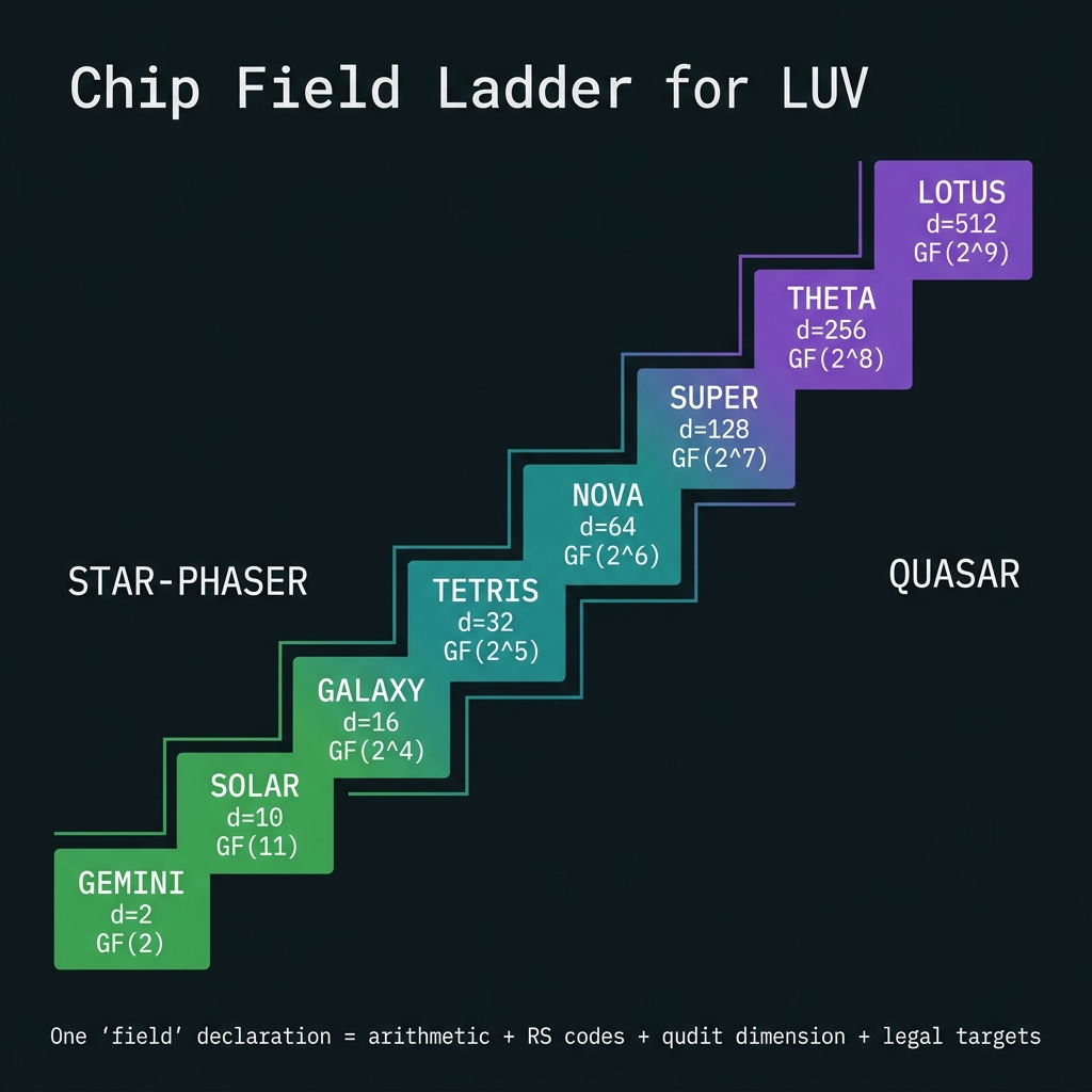 Field ladder
field declaration fixes arithmetic, RS codes, qudit dimension, and legal targets across the entire chip ladder.GEMINI — Clements mesh
mesh dft N synthesizes exact unitaries via Clements 2016 decomposition. 28 active phases project to a 32-channel AD5372 DAC vector with crosstalk correction [model].
SOLAR → LOTUS — QFP gates
gate X_d/Z_d/F_d D composes into a QFP schedule. Holograms lower to phase masks; v0.3 hologram time expands to slot-tagged TDM steps for rank-2 programs on LOTUS.
Three timing tiers the language already encodes
LUV targets the artifact contract; the FPGA (or ASIC scheduler) consumes it. The simulator's stall semantics are the behavioral spec for future firmware.
| Tier | Latency | LUV surface | Hardware path |
|---|---|---|---|
| Feedforward | ~11.2 ns | when after measure |
SPAD → 64 ps TDC → FPGA BRAM lookup → TFLN EO switch. Photon held in 3.5 ns delay spiral. |
| Reconfiguration | ~54 µs | mesh, phases, DAC vector |
FPGA → SPI → AD5372 → 32 heaters. Heater τ_rise ≈ 1 ms dominates settling. |
| Environment | <30 s → ~16 min | comb_lock.grid_valid |
L0 TEC → L1 band heaters → L2 per-tooth servo. grid_valid is the hardware interlock — sequencer refuses opcodes when comb is not locked. |
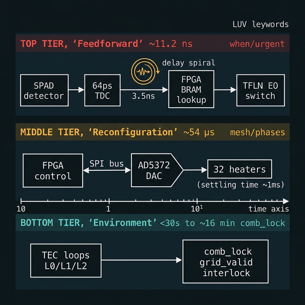 Timing tiers
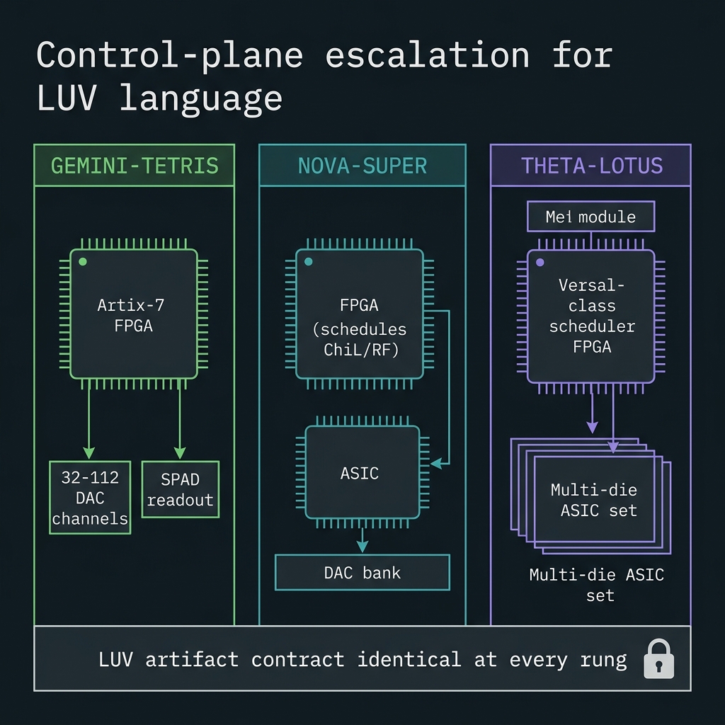
FPGA means different things at each rung
On GEMINI–TETRIS, the Artix-7 FPGA is the control brain (32–112 DAC channels, SPAD readout). From NOVA upward, a companion ASIC owns the DAC bank while the FPGA schedules ChiL/RF. At THETA/LOTUS, a Versal-class scheduler orchestrates a multi-die ASIC set. LUV is insulated from this escalation — the artifact contract is identical at every rung.
Acceptance test = luvc run
When FPGA firmware exists, its acceptance test is byte-level agreement with the digital twin. Post-selection bookkeeping, measure-destructuring rules, and grid_valid stall semantics are already encoded in the simulation layer [simulated].
GEMINI: Artix-7 + 2× AD5372 · 24 SPAD → 64 ps TDC
 Control plane
What the compiled bundle actually contains
Every luvc build emits a .qil.json bundle — a single JSON file containing the full intermediate representation, hardware artifacts, and honesty metadata. This is the contract between the compiler and the execution layer.
Intermediate Representation
Version-stamped "0.1.0", chip target, backend (sim or qpu), and an ordered array of IROperation objects. Each operation has a kind (from the OpKind enum), params, modes, and an honesty label.
Three Hardware Contracts
dac.voltages[] — crosstalk-corrected heater voltages via G⁻¹ inverse thermal matrix.qfp_schedule[] — ordered unitary/phase-mask/permute steps.shot_contract — SPAD herald pattern + post-selection probability.
Honesty + Provenance
Every tier carries "honesty" as a structural JSON field. gf_k (field exponent), emits (debug outputs), rs_ok (syndrome pass/fail), feedforward_ops (kept separate from pre-shot schedule).
Six Verilog modules that close the loop
The GEMINI control plane is implemented as six RTL modules targeting Artix-7 XC7A100T at 200 MHz. These modules consume the three QIL artifacts and drive the photonic chip in real time. [designed/target]
Top module
Integrates all subsystems with a memory-mapped register file. Register map: CTRL, STATUS, N_FRAMES, STALL_COUNT, FF_ADDR/DATA, MEAS, PATTERN. Coordinates the three timing tiers and exposes a USB-UART debug port to the STM32H7 supervisor MCU.
DAC SPI master
Drives 2× AD5372 (64 channels) in parallel SPI. Init: CLR high → RESET pulse → wait BUSY. Per refresh: 24-bit X-write frames at ≥600 ns SYNC pitch → wait BUSY → LDAC pulse (≥10 ns). Stall semantics: refuses refresh when grid_valid is LOW — mirroring run_freqbin_shot.
BRAM feedforward LUT
16k × 64-bit BRAM lookup table. Each LUV when line compiles to exactly one row. Address = decoded measure value, data = 64-bit TFLN switch-tree mask. Registered BRAM read: 2 clock cycles from meas_valid to mask_valid. At 200 MHz: 2 cycles = 10 ns [model].
Time-to-digital converter
24-channel time tagger with 64 ps LSB (model stand-in for carry-chain TDC). 35 ns dead time per channel. Outputs Swabian-style (channel, t64) timestamp tags with exponentially modified Gaussian jitter model. 33-bit words, LVDS interface.
Herald coincidence filter
Accepts timestamp streams from tdc_capture, applies |Δt| < 128 ps coincidence window between herald and mesh detectors, outputs sticky click pattern. This is the gate between photon detection and classical post-processing.
Comb-lock opcode gate
Hardware interlock that refuses all opcode issue when the comb servo is not locked. Three lock levels: L0 (TEC stable), L1 (band heaters converged), L2 (per-tooth servo locked). grid_valid = (level == L2). Exactly mirrors run_freqbin_shot stall semantics.
How one SPAD click rewrites the photonic circuit in nanoseconds
0.0 ns — A heralded photon hits the InGaAs SPAD (Aurea, PDE ≥ 28%). The avalanche produces a ~1 ns electrical pulse.
1.0 ns — The TDC latches the click with 64 ps time resolution, producing a (channel, t64) tag. The coincidence filter checks the herald window.
1.5 ns — The decoded measure value (bin index → GF symbol) is presented to the feedforward LUT address port.
~6.0 ns — Registered BRAM read completes (2 × 5 ns at 200 MHz). The 64-bit switch-tree mask is valid on the LUT output.
~6.5 ns — Mask drives the TFLN electro-optic switch array. Sub-nanosecond EO switching; the frequency-bin grid shifts or a Z_d phase gate is applied.
~11.2 ns total — Complete. The partner photon, held in a 3.5 ns on-chip SiN delay spiral, exits the modified circuit with the correction already applied.
This is why LUV exists as a device language: the when keyword doesn't just describe conditional logic — it describes a nanosecond-scale physical feedback loop that rewrites the photonic circuit between the detection of one photon and the release of its entangled partner.
The digital twin that defines firmware behavior
luvc run executes LUV programs against a physics-accurate simulation. This simulation is not just a development aid — it is the formal behavioral specification for all future FPGA and ASIC firmware.
Gaussian states → torontonian detection
For GEMINI's spatial Clements mesh: Mr Mustard (Xanadu) builds a Gaussian state — two-mode squeezed vacuum through a beamsplitter mesh keyed to the 28 Clements phases, with attenuation from chip wiring parameters. The Walrus computes the torontonian to draw threshold SPAD events across 24 channels. Returns {"honesty": "[simulated]/[model]", "spad_pattern": [...], "phases": [...]}.
WDM Gaussian states → bin readout
For SOLAR through LOTUS: initializes uniform amplitude across d frequency bins, applies the QFP schedule via apply_qfp_schedule(amp, schedule), records per-slot amplitudes for TDM programs, reports post_selection_prob (surviving norm² for non-unitary masks). Critical: enforces comb_lock.grid_valid before issuing any gate — if the comb servo is not locked, the shot stalls and returns {"ok": false, "stalled": true}.
How SPAD clicks become GF symbols
Frequency-bin path: the detector click lands in one of d bins; the symbol is argmax(|qfp_amplitude|) — deterministic in simulation, probabilistic on hardware. The integer bin index is the GF element.
Mesh path: GEMINI's 24-SPAD bit pattern has its first k bits packed little-endian into a GF(2k) symbol. On GEMINI (k=1), this is a single bit — qubit measurement.
grid_valid — the hardware interlock
Three lock levels modeled in comb_lock.py: L0 (TEC substrate stable), L1 (band heaters converged), L2 (per-tooth servo locked, all teeth within ±5 MHz of grid). grid_valid = (level == "L2"). The DQFP sequencer refuses opcode issue when the comb servo is not locked — exactly as run_freqbin_shot stalls in simulation. [model] steady-state lock proxy, no loop dynamics.
What the test suite validates
test_luv.py (121 tests)
Parser validation, glyph/ASCII equivalence, GF constant folding (AES vector: 0x57 × 0x83 = 0xC1 under GF(2⁸)), RS round-trip encode/decode, full E2E: parse → lower → compile → DAC → shot → measure → feedforward.
test_solar_track.py
Comb lock: zero detuning → L2/grid_valid=true; 80 MHz detuning → L1; 500 MHz → stall. Verifies the stack refuses herald patterns when spectral grid is out of spec.
test_fpga_firmware.py
12 acceptance tests across 5 suites: DAC SPI frame byte-exact match, TDC timestamp format, coincidence window, feedforward BRAM lookup, grid_valid interlock. Behavioral spec for RTL.
What exists today
No FPGA firmware is shipped. All execution results are digital-twin output until hardware bring-up.
Digital twin
Numbers produced by galois/JAX simulation: heralded shots, torontonian detection, exact Clements synthesis, freq-bin gate composition.
Engineering approximation
Hardware-subset 28-phase projection, thermal crosstalk matrices, AD5372 voltage encoding, feedforward latency budget.
Design intent
Chip specifications, DAC channel counts, timing budgets, and control-plane architecture — unverified against silicon.
| Version | Highlights | Status |
|---|---|---|
| v0.1 | mesh, shot, GEMINI path | Shipped |
| v0.2 | Array verbs (⌽, ⍉, iota), RS codec, freq-bin gates, measure | Shipped |
| v0.3 | hologram time (TDM), when feedforward, QFP→heater DAC lowering, AD5372 SPI frames | Current — 121-test suite green |
Explore the LUV toolchain
LUV is released for internal and partner circulation. The compiler, 121-test suite, VS Code syntax extension, and seven example programs are available in the QIL stack.