Three phases to a vertically integrated quantum photonic chip fab
QLT is pursuing a phased strategy to build a vertically integrated quantum photonic chip fabrication facility in a Texas Opportunity Zone — capturing federal and state tax incentives worth tens of millions while establishing sovereign US manufacturing for quantum hardware.
From $25M split-fab prototype to $1.2B sovereign manufacturing
QLT's manufacturing strategy is a disciplined three-phase path: prove the physics and lock down IP with a split-fab prototype ($25M), build a dedicated pilot facility ($150M), then scale to a full vertically integrated fab ($1.2B). Each phase is milestone-gated and de-risks the next.
Three phases from first silicon to volume production
Split-Fab Prototype + IP Fortress
5 strategic seats × $5M each. Pillar 1: $5M split-fab prototype across Ligentec, AIM Photonics, and imec with encrypted partial GDS. Pillar 2: $20M IP expansion — 60+ patent families across 7 jurisdictions with defensive litigation reserves.
Pillar 1: $5M prototype · Pillar 2: $20M IP · 3–5 FTE · 12–18 months
Dedicated Pilot Fab
Purpose-built 25,000–30,000 sq ft facility with 10,000–15,000 sq ft ISO 5–7 cleanroom. DUV stepper ($8–12M), dual ICP-RIE etchers, PECVD/LPCVD for SiN, e-beam lithography, full metrology suite, fiber-attach packaging. Texas Opportunity Zone.
$80M equipment · $32M facility · $13M team · 25–30 FTE · 10–20 WPW
Full-Scale Vertically Integrated Fab
World-class quantum photonic chip fabrication facility. 50,000+ sq ft, DUV lithography, FOUP-based automation, MES-integrated production, AI-driven fault detection, advanced packaging lines, integrated quantum test lab. Lights-out 24/7 manufacturing.
200/300mm wafer class · 50–80+ FTE · Thousands of WPY · IPO-ready
Process-aligned equipment for full-stack quantum photonic chip production
Every piece of equipment below maps directly to a step in QLT's 9-step fabrication process traveler — from bare Si₃N₄ wafer to packaged, tested, fiber-coupled quantum photonic processor. This is the complete production pipeline.
Wafer Fabrication & SiN Core Deposition
5 Systems · $18–25MLPCVD Furnace (Si₃N₄)
→Deposits the stoichiometric silicon nitride waveguide core layer via LPCVD. Dichlorosilane + ammonia at ~800°C produces ultra-low-loss Si₃N₄ with precise thickness control (±2nm uniformity).
Tempress / ASM · 200mm capacity · 3-zone · ≤0.5% uniformity
$3–5M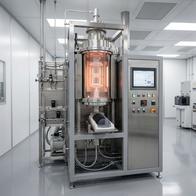
PECVD System (SiO₂)
→Deposits SiO₂ upper cladding at low temperature (~300°C) using TEOS/O₂ chemistry. Provides the symmetric refractive index environment required for fundamental mode confinement.
Oxford Instruments / Applied Materials · 200mm · TEOS + O₂
$2–4M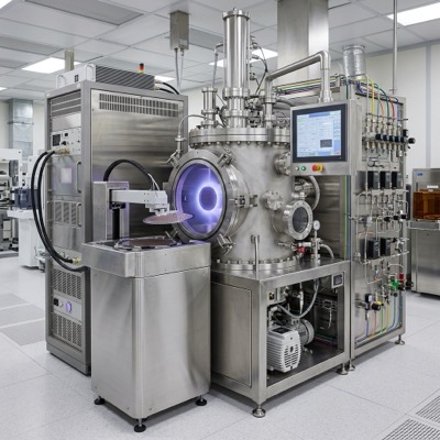
CMP System
→Chemical-mechanical planarization achieves <5nm surface roughness on the SiO₂ cladding — critical for bonding the proprietary ODR overlay material.
Strasbaugh / Logitech · 200mm · sub-nm roughness target
$2–4M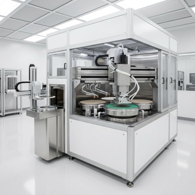
Thermal Oxidation Furnace
→Grows the 4 µm thermal SiO₂ buried oxide (BOX) layer on bare silicon wafers. Prevents optical mode leakage into the silicon substrate.
Lindberg / Tempress · O₂/H₂O ambient · 1100°C max
$1–2M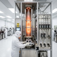
ALD System
→Atomic layer deposition of ultra-thin Al₂O₃ interlayers (~5nm) for bonding interfaces, passivation, and etch-stop layers.
Cambridge Nanotech / Beneq · 200mm · TMA + H₂O
$1–2M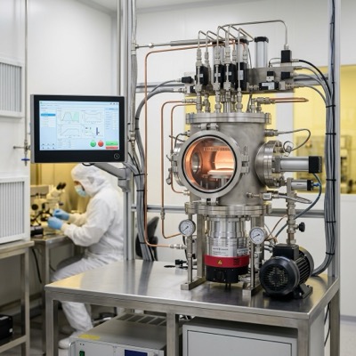
Lithography — Pattern Definition
3 Systems · $12–18MDUV Stepper/Scanner (248nm)
→Primary production lithography for all waveguide layers, grating coupler patterns, MZI mesh routing, and alignment marks. 248nm KrF achieves resolution for all photonic features ≥180nm.
Canon FPA-3000 or Nikon NSR · 248nm KrF · ≤180nm resolution · 200mm
$8–12M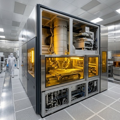
E-Beam Lithography System
→Writes proprietary ODR waveguide structures — nano-scale geometries requiring sub-50nm edge placement precision. Also used for prototype mask generation.
JEOL JBX-9500 · <10nm beam · 100kV · stitching <20nm
$3–5M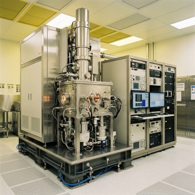
Resist Track (coat/develop)
→Automated spin-coat, soft-bake, develop, and post-bake of photoresist. Ensures uniform ~1.5µm resist thickness (±1%) for consistent exposure dose.
TEL / DNS · 200mm · programmable recipes
$1–2M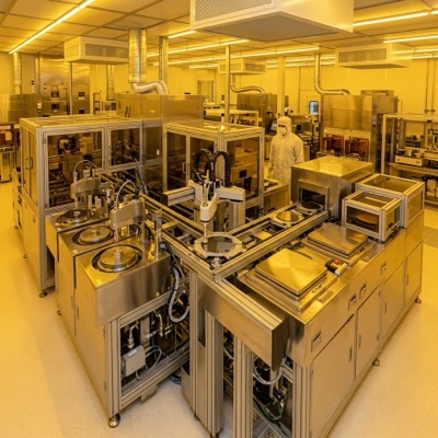
Dry Etch — Waveguide & Trench Formation
3 Systems · $6–10MDual ICP-RIE System
→Primary etch tool. Chamber 1: CHF₃/O₂ etches SiO₂ cladding for trench windows. Chamber 2: CHF₃/Ar/O₂ etches Si₃N₄ waveguide channels with ultra-smooth sidewalls.
Oxford PlasmaPro 100 / PlasmaTherm · dual chamber · ICP + RIE · 200mm
$4–8M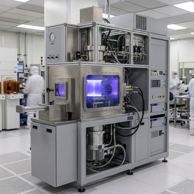
O₂ Plasma Asher/Descum
→Post-etch oxygen plasma clean removes resist residue and passivates etch-damaged surfaces. Critical for clean Si₃N₄ surface.
Technics / Diener · barrel or downstream · O₂ at 200W
$200–500K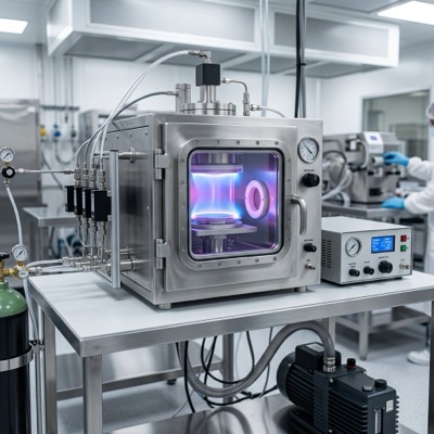
Wet Bench Suite
→Solvent clean, piranha clean (H₂SO₄:H₂O₂), buffered HF for precision oxide thinning, and MF-319 developer. Separate benches for acids, solvents, and DI rinse.
Wafer-Process / custom · acid-resistant · recirculating DI · fume hood
$500K–1M
ODR Overlay & All-Optical Switch Integration
4 Systems · $4–7M · PROPRIETARYProprietary Overlay Evaporator
→Deposits the proprietary ODR overlay material onto waveguide sections using controlled thermal evaporation for efficient on-chip coherence restoration.
Custom / Denton · 3-pocket · base pressure <5×10⁻⁶ Torr · rate ~1 Å/s
$1–2M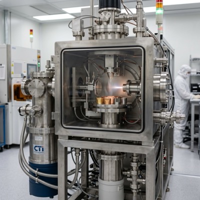
PVD Sputter System
→Alternative overlay deposition path and metal seed layers (Ti/TiN) for electrode adhesion. Magnetron sputtering provides uniform trench sidewall coverage.
AJA / CHA · multi-target · RF/DC magnetron · 200mm
$1–2M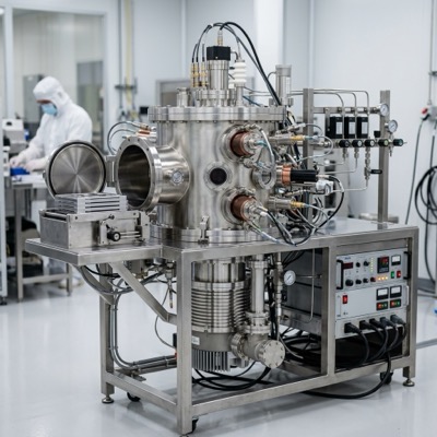
Precision Micro-Assembly Station
→Manual pick-and-place of prefabricated all-optical switch nano-stacks into etched waveguide trenches. Requires ±200nm alignment accuracy.
Custom station · ≥200× microscope · 6-axis manipulator · ±0.2µm
$500K–1M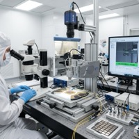
Flip-Chip Bonder
→Automated precision bonding of LiNbO₃ thin-film components to Si₃N₄ PIC. Direct bonding at 250°C creates permanent hybrid waveguide structure.
SUSS FC150 / SET FC300 · ±1µm accuracy · force + temp control
$1–2M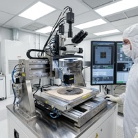
Metallization, Anneal & Passivation
3 Systems · $3–5ME-Beam Evaporator
→Deposits Ti/Au metal stack by electron-beam evaporation. Ti (30nm) provides adhesion; Au (200nm) forms low-resistance electrodes and all-optical switch mirrors.
Denton Nexdep / CHA · 3-pocket · planetary rotation · crystal monitor
$1–2MForming Gas Anneal Furnace
→Post-metallization anneal at 425°C in 95:5 N₂/H₂ for 90 minutes. Hydrogen passivates dangling bonds, reducing optical absorption.
Lindberg / Tempress · 3-zone tube · N₂/H₂ forming gas · ≤1100°C
$500K–1M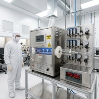
RTP (Rapid Thermal Processor)
→Quick thermal anneals for dopant activation, contact sintering, and stress relief. 10-second spike profiles minimize thermal budget.
AG Associates / Mattson · 200mm · <50°C/s ramp · N₂/O₂ ambient
$500K–1M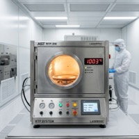
Dicing, Fiber Attach & Packaging
5 Systems · $8–12MAutomatic Dicing Saw
→Singulates 7×7mm photonic dies from 200mm wafer. 50µm diamond blade, coolant-assisted to prevent thermal damage to ODR overlay.
DISCO DAD-3220 · 200mm · auto-alignment · ±5µm accuracy
$1–2M
6-Axis Fiber Alignment + IR Camera
→Precision end-fire coupling of PM fiber arrays to chip facets. Sub-micron active alignment via IR camera feedback.
PI P-611 NanoCube / Newport · 6-DOF · sub-µm · PM fiber V-groove arrays
$1–2M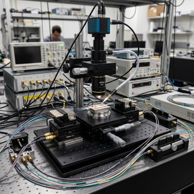
Wedge Wire Bonder
→Bonds 25µm gold wire from chip pads to ceramic carrier at ~120g force, 120ms ultrasonic. Connects electrodes, heaters, SPAD bias pads.
K&S 4523 / West-Bond · 25–50µm Au/Al · wedge + ball modes
$500K–1M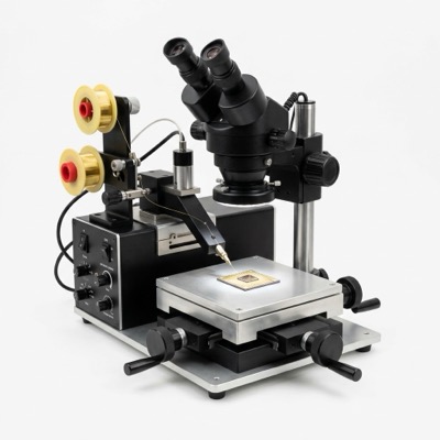
Hermetic Packaging Line
→Vacuum oven with getter material for seam-seal. Dry nitrogen atmosphere. Butterfly or QSFP-compatible form factor.
Vacuum oven + lid sealer · N₂ purge · getter · epoxy or seam-seal
$1–2M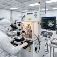
Advanced Packaging (Phase 3 prep)
→Flip-chip bonding, TSVs, and 2.5D interposer integration for multi-chip quantum processor modules.
Automated die attach · TSV processing · interposer bonding
$2–3M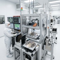
Metrology, Characterization & Quantum Test Lab
7 Systems · $12–18MSEM (Scanning Electron Microscope)
→Sub-nm imaging of waveguide sidewalls, photonic crystal hole profiles, trench dimensions. In-line process control for etch recipe optimization.
FEI / Hitachi · field-emission · <2nm resolution · 200mm stage
$2–4M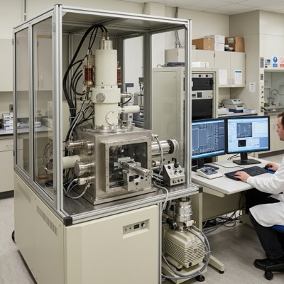
AFM (Atomic Force Microscope)
→Surface roughness measurement on CMP-polished cladding, ODR overlay film quality, and bonding interface inspection.
Bruker Dimension / Park · tapping mode · <0.1nm z-resolution
$500K–1M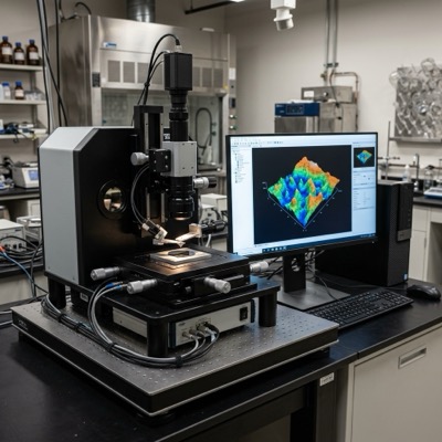
Spectroscopic Ellipsometer
→Non-destructive measurement of Si₃N₄ film thickness (±2nm) and refractive index across full wafer.
J.A. Woollam / HORIBA · 190–1700nm · 200mm mapping
$500K–1MAutomated Wafer-Level Optical Prober
→Tests every die on-wafer before dicing: waveguide loss, MZI extinction ratio, ring resonator Q-factor.
Keysight / FormFactor · tunable laser 1500–1600nm · fiber array probe
$2–4M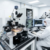
High-Speed Detector + ESA
→Characterizes all-optical switch timing: femtosecond switching speed, extinction ratio, and jitter validation.
u²t / Finisar 50 GHz PD · Keysight N9040B ESA · pulsed laser source
$2–3MSingle-Photon Detectors (SPADs)
→Room-temperature quantum herald measurements: single-photon generation, path entanglement, Hong-Ou-Mandel dip visibility.
Excelitas / ID Quantique · Si SPAD + InGaAs SPAD (1550nm) · <100ps jitter
$1–2M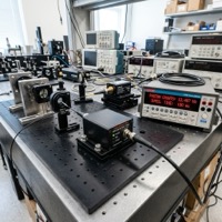
OSA + Tunable Laser
→Measures ODR conversion efficiency, waveguide spectral response, grating coupler bandwidth, and parasitic reflection levels.
Yokogawa AQ6370 OSA · Santec TSL-570 tunable laser · 1500–1620nm
$500K–1MFacility Shell, Cleanroom & Infrastructure
7 Systems · $30–38MHVAC/HEPA Filtration
→Laminar flow, temperature ±0.1°C, humidity ±1% RH in lithography bay
ISO 5–7 cleanroom · HEPA/ULPA · 10K–15K sq ft
$4–6M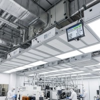
Vibration Isolation
→Active isolation pads for DUV stepper and e-beam writer (VC-D or better)
TMC / Herzan · active pneumatic · VC-D compliance
$1–2M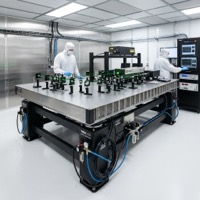
Power & UPS
→Redundant 3-phase 480V service, 500 kVA UPS, generator backup
Eaton / APC · 500 kVA · dual-feed · generator
$2–3M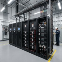
UHP Gas Delivery
→CHF₃, SF₆, O₂, N₂, Ar, forming gas — double-contained lines with gas monitoring
Matheson / Praxair · double-contained · gas monitoring
$2–3MDI Water + Chemical Waste
→18.2 MΩ DI water system, chemical waste treatment, acid neutralization
Millipore / Evoqua · 18.2 MΩ · acid neutralization
$1–2MMES + Automation + IT
→Manufacturing Execution System, recipe management, yield analytics, FOUP handling, facility monitoring
Custom MES · SECS/GEM · automated FOUP handling
$3–5M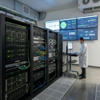
Safety & Security
→Gas monitoring, FM-200 fire suppression, SCBA, CCTV, card access, EHS, ITAR-compliant zones
FM-200 · gas detection · ITAR restricted access
$2–3M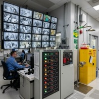
10–20 wafers per week · yielding 50–200+ packaged quantum photonic processors per week · first revenue within 12–18 months of facility commissioning
Texas Opportunity Zone + federal incentives
Layered incentive stack worth $30–50M+ in tax savings
By locating the pilot fab in a Texas Qualified Opportunity Zone, QLT can layer federal and state tax programs to reduce effective facility cost by 20–35%. Texas has 628 designated OZ tracts across 145 counties — including census tracts adjacent to Samsung (Taylor/Austin), Texas Instruments (Dallas/Richardson), and established semiconductor corridors near San Antonio.
Texas also has no state income tax, no state capital gains tax, and an active semiconductor-specific incentive ecosystem established by the Texas CHIPS Act (HB 5174) and the Texas Quantum Initiative (HB 4751).
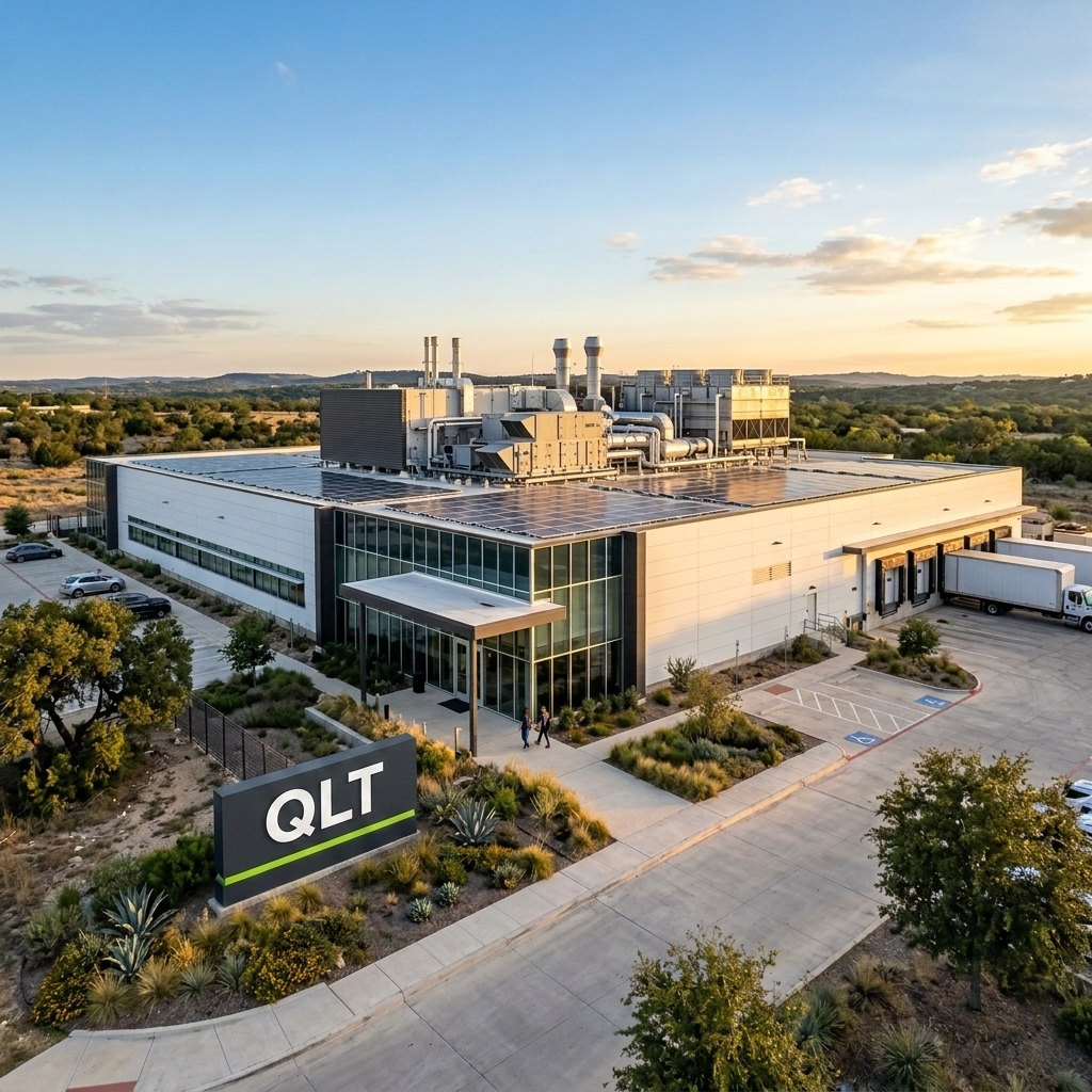
Projected pilot fab · Texas Opportunity Zone · 30,000 ft²
Tax-free appreciation on 10-year hold
- Capital gains invested in a Qualified Opportunity Fund (QOF) are deferred for 5 years
- 10% basis step-up after 5 years (30% for qualified rural OZ funds)
- All appreciation on the QOF investment is 100% tax-free if held 10+ years
- Program made permanent by the 2025 "One Big Beautiful Bill Act" — OZ 2.0 effective Jan 1, 2027
- On a $150M pilot facility, 10-year tax-free appreciation could shelter tens of millions in gains
Property tax abatement + 25% OZ bonus
- 10-year limitation on school district M&O appraised value (50% abatement)
- Additional 25% bonus abatement for projects in Qualified Opportunity Zones
- Effective 75% school property tax reduction for 10 years in an OZ
- Eligibility: advanced manufacturing with $20–200M investment + 10–75 jobs (by county)
- Must pay 110% county average wage and provide health benefits
Semiconductor Innovation Fund (TSIF)
- Texas Semiconductor Innovation Fund provides grants for in-state R&D and manufacturing
- Federal CHIPS Act provides direct subsidies for domestic semiconductor manufacturing
- Texas Enterprise Fund available as "deal-closing" grant for projects competing with out-of-state locations
- Sales and use tax exemptions on manufacturing equipment purchases
Estimated incentive value on $150M pilot fab
| Incentive Program | Mechanism | Estimated 10-Year Value |
|---|---|---|
| Federal Opportunity Zone 2.0 | Capital gains deferral + tax-free appreciation after 10yr hold + 10% basis step-up at 5yr | $10‑25M+ (depends on appreciation) |
| Texas JETI Act (base) | 50% school district M&O property tax abatement for 10 years | $5‑12M |
| Texas JETI OZ Bonus | Additional 25% abatement for OZ-located projects (total 75%) | $3‑6M |
| Texas Sales Tax Exemption | Manufacturing equipment exempt from 6.25% state + local sales tax | $5‑8M |
| Federal CHIPS Act Grants | Direct subsidies for domestic semiconductor manufacturing | $5‑15M+ (application-dependent) |
| Texas Enterprise Fund | "Deal-closing" discretionary grant from Governor's office | $1‑5M |
| No State Income / Capital Gains Tax | Texas has zero state income tax and zero capital gains tax | Ongoing (structural savings) |
| Total Estimated Incentive Value | $30–70M+ over 10 years |
Tax incentive estimates are preliminary and subject to qualification, application, and regulatory processes. Consult tax and legal advisors for specific investment guidance.
Why QLT builds its own fab
Absolute process control
The ODR overlay, proprietary all-optical switch integration, and advanced waveguide processing are QLT's core differentiators. In-house fabrication eliminates IP exposure risk entirely. No encrypted GDS, no NDAs, no split manufacturing — full physical custody of every wafer.
Weeks, not months
External foundry cycles take 3–6 months per run. An in-house fab reduces prototype iteration to 2–4 weeks — critical for tuning ODR conversion efficiency, proprietary switch geometry, and process window optimization during development.
US-sovereign manufacturing
Defense and intelligence customers require ITAR-compliant, US-based fabrication. A domestic fab qualifies QLT hardware for DoD Trusted Foundry programs, SBIR/STTR partnerships, and classified quantum applications that require full chain-of-custody.
From wafer to packaged product
The facility covers the full stack: lithography, etch, deposition, post-processing, packaging, fiber-attach, test, and qualification. No dependency on external assembly houses or packaging vendors for the complete product.
Revenue from excess capacity
Excess fab capacity can serve external customers as a US-based photonic foundry — filling an unmet market need for domestic SiN fabrication with advanced integration capabilities. This mirrors Infinera's strategy of vertical integration as a competitive moat.
$30–70M+ in captured incentives
Texas OZ location + JETI Act + CHIPS Act + sales tax exemptions + zero state income tax compounds to reduce effective facility cost by 20–35%, making the $150M Series A investment comparable to a $100M facility in tax-advantaged terms.
42-week plan to first silicon
The immediate path uses commercial foundry runs while building proprietary post-processing capability in parallel.
Design & Layout
PIC design, DRC verification, mask layout review using the universal checklist, MPW submission to Ligentec AN350.
Foundry Fabrication
Split-fab across multiple foundries (Ligentec, AIM Photonics, imec) with encrypted partial GDS. No single vendor sees the full design. In parallel: set up NDA-controlled clean environment for ODR overlay and final assembly.
Post-Processing & Assembly
In-house ODR overlay (proprietary waveguide processing), all-optical switch integration, die singulation, facet polishing, and micro-assembly.
Packaging & Fiber Attach
Wire bonding, fiber alignment, encapsulation, lid sealing, and initial electrical/optical verification.
Test & Validation
Full integrated test plan: waveguide loss, ODR conversion efficiency, all-optical switch timing, MZI fidelity, and first quantum herald measurements.
Two-pillar investment structure
- Split-fab MPW runs (Ligentec, AIM, imec): $1M
- Multi-foundry IP protection (encrypted GDS): $1.2M
- Patent prosecution (34+ filings): $1M
- R&D + simulation (Lumerical, Ansys): $800K
- Team + ops (3–5 FTE, 12 months): $1M
- Patent portfolio expansion (60+ families): $8M
- International protection (7 jurisdictions): $5M
- Defensive litigation & enforcement: $5M
- Trade secret & data infrastructure: $2M
Complete manufacturing stack
QLT has prepared: fabrication-ready build schematic (AN350), 42-week GANTT chart, process traveler and test plan, mask layout checklist, foundry selection workflow, proprietary switch integration protocol, and full equipment procurement checklists.
Eight per-chip manufacturing processes (WS14)
Complete start-to-finish travelers: layer recipes, metrology gates, yield engineering — one page per chip.
Discuss the manufacturing strategy and facility investment
QLT is seeking partners and investors who understand US-sovereign quantum hardware manufacturing. The Texas Opportunity Zone strategy creates a structural tax advantage that amplifies every dollar invested.